PSU Reversing Part 1
I’m waiting on a variac I’m borrowing from another lab member before I can start bringing up the PSU, so I started reverse engineering the linear board of the power supply into a schematic this evening. This is partly to help with any required troubleshooting, and partly (mostly) since I want to understand how it works better. The board has a lot of parts that I wouldn’t have expected on it, such as SCRs and large numbers of high-power wirewound resistors, and I want to understand what all of them are there for.
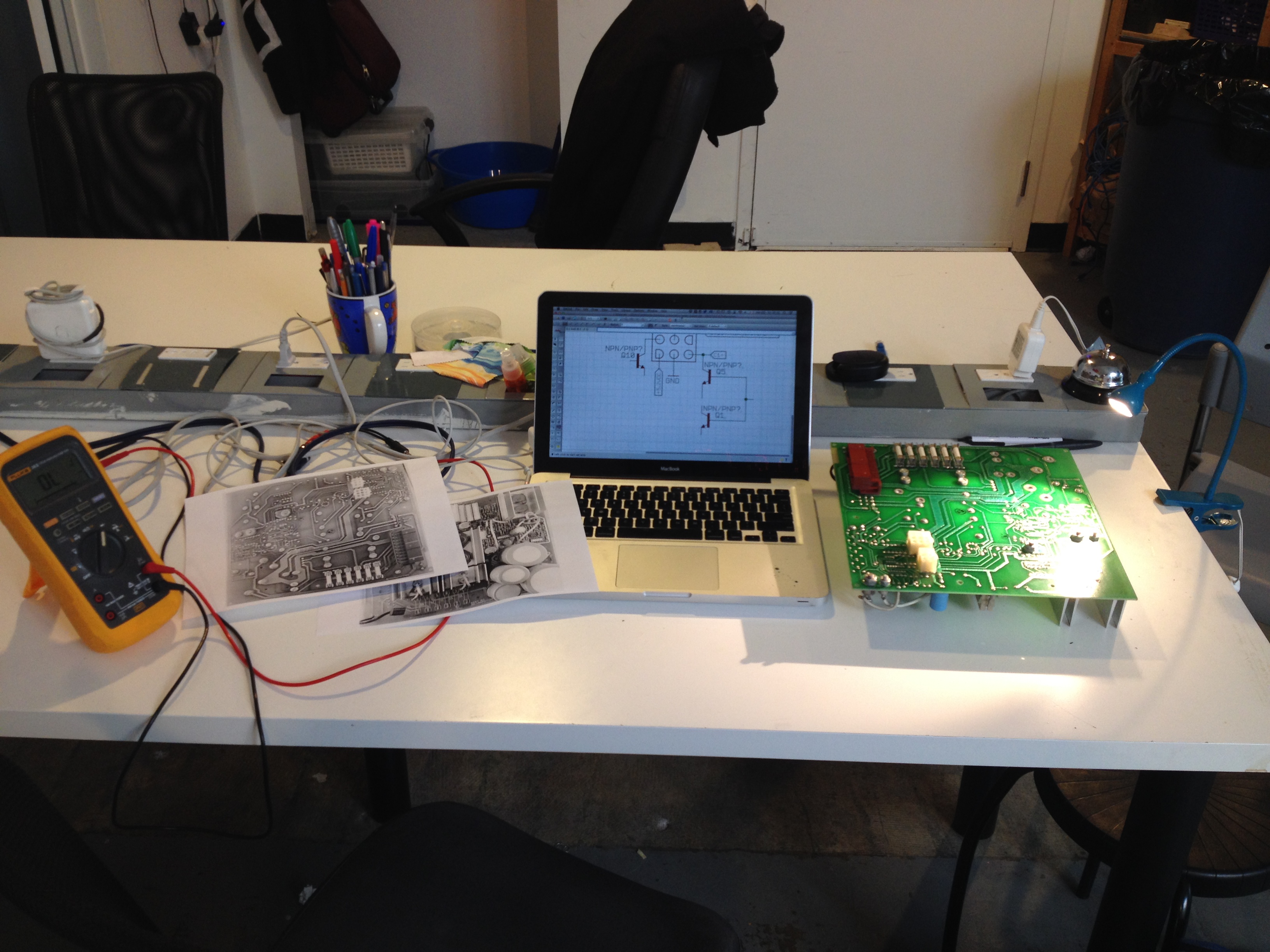
Working on reversing the PSU at HackLab.TO.
Reverse engineering older power stuff like this is not that difficult overall, just tedious at times. It’s a double-sided board, no ground planes, and mostly fairly thick traces, so following traces around isn’t that hard. All the components are through-hole (or bolt-on, in the case of the big power parts), so reading values off (most of) the passives is easy too.
I started by taking some good shots of the board, turning them to B&W and increasing the contrast, then printing out one of each side of the board. I found a fairly random spot to start (the first transformer tap input) and followed where the trace went, drew that into the schematic, and marked it off on the paper copy to show it’s been transcribed. Then repeated that for the next few hours. When traces go under other parts, a combination of bright light through the board and my multimeter on continuity mode helps find where they go, and I took the big caps off the board to help with that too, since they just unbolt.

Tracking sheet I use to mark off each trace that’s put into the schematic, after the first few hours of reversing.
The hardest part so far is that most of the components have Xerox-specific part numbers on them, so I can’t just look up datasheets to find pinouts. TO-3 transistors have a fairly standard pinout, so I’m assuming they use that one until I get the schematic a bit more complete. I’m still not sure if they’re PNP or NPN, but as more of the schematic gets completed it should become more obvious which they are, as should the pinout.
Thankfully the crowbar chips have the original part numbers (MC3423) which lead me to a datasheet. This finally explained what all the SCRs on each board are for, which is to crowbar the supply in case of overvoltage, not power sequencing on startup like we’d guessed. If the voltage on a rail goes too high, the crowbar chip triggers the SCR to short out the voltage rail and blow the fuse.
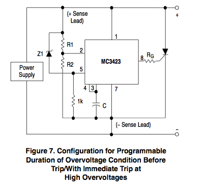
An example schematic of how the MC3423 can be used, which was helpful in figuring out what the designers were doing.
At this point the connectors, a small part of the rectification/regulation circuitry, and the crowbar circuitry for the +24V rail is reversed out. Since this board has 4 rails and 4 of the crowbar controller chips, the next 3 crowbars should be easy to reverse, just copy/pasting in EAGLE and beeping out each trace to confirm that it matches the same design.
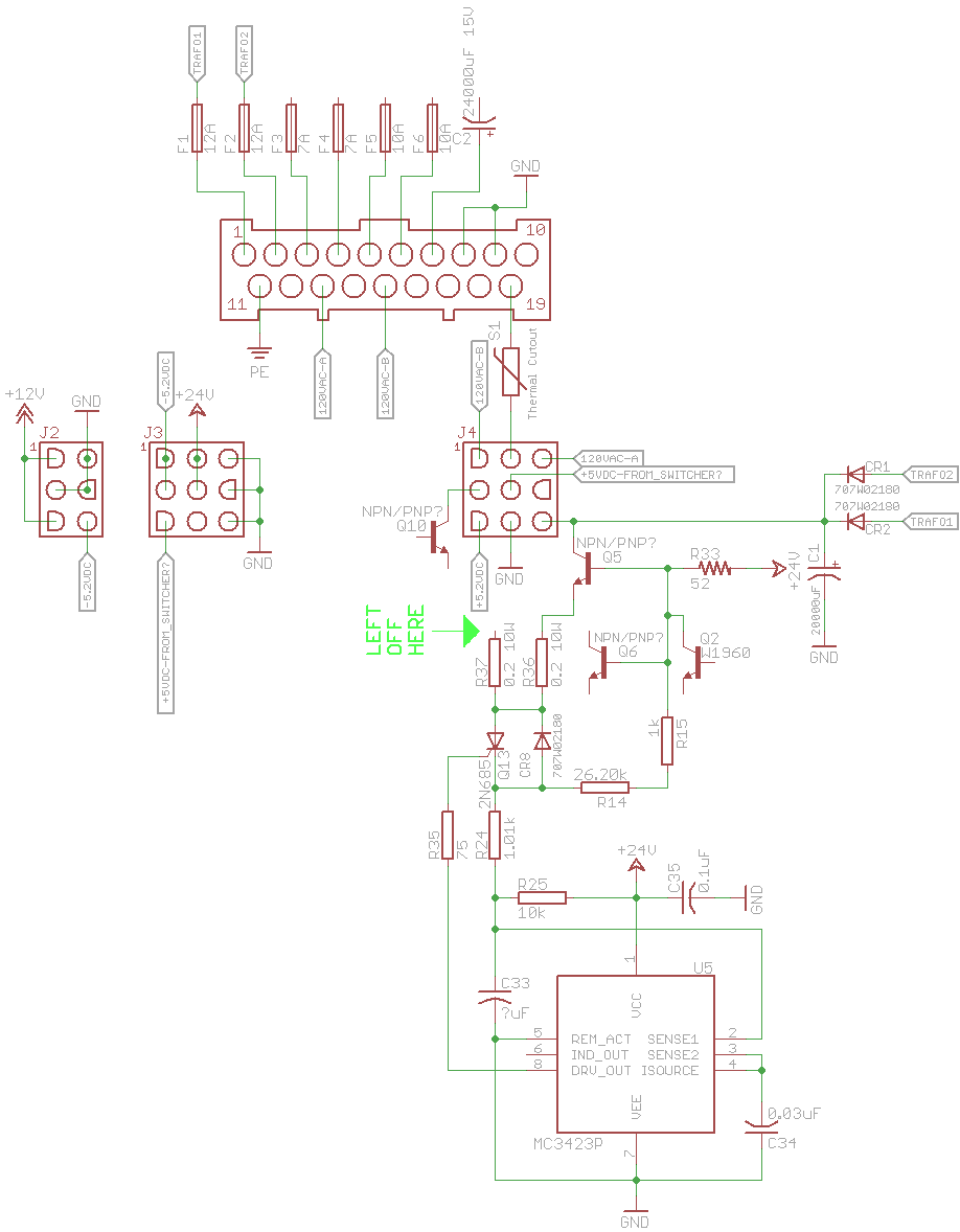
The schematic of the PSU’s linear board at the end of the first few hours of reversing.
Leave a Reply